- 您现在的位置:买卖IC网 > Sheet目录3880 > PIC18F8621T-I/PT (Microchip Technology)IC PIC MCU FLASH 32KX16 80TQFP
2005 Microchip Technology Inc.
DS39612B-page 9
PIC18F6525/6621/8525/8621
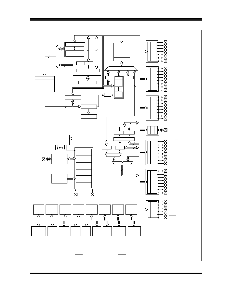
FIGURE 1-1:
PIC18F6525/6621 BLOCK DIAGRAM
Power-up
Timer
Oscillator
Start-up Timer
Power-on
Reset
Watchdog
Timer
Instruction
Decode and
Control
OSC1/CLKI
OSC2/CLKO
VDD,
PORTA
PORTB
PORTC
RA4/T0CKI
RA5/AN4/LVDIN
RB0/INT0/FLT0
RC0/T1OSO/T13CKI
RC1/T1OSI/ECCP2(1)/P2A(1)
RC2/ECCP1/P1A
RC3/SCK/SCL
RC4/SDI/SDA
RC5/SDO
RC6/TX1/CK1
RC7/RX1/DT1
Brown-out
Reset
RA3/AN3/VREF+
RA2/AN2/VREF-
RA1/AN1
RA0/AN0
Timing
Generation
RB1/INT1
Data Latch
Data RAM
(3.8 Kbytes)
Address Latch
Address<12>
12
Bank 0, F
BSR
FSR0
FSR1
FSR2
inc/dec
logic
Decode
4
12
4
PCH
PCL
PCLATH
8
31 Level Stack
Program Counter
PRODL
PRODH
8 x 8 Multiply
W
8
BITOP
8
ALU<8>
8
Test Mode
Select
Address Latch
Program Memory
(48/64 Kbytes)
Data Latch
20
21
16
8
Table Pointer<21>
inc/dec logic
21
8
Data Bus<8>
Table Latch
8
IR
12
3
ROM Latch
PORTD
RD7/PSP7
RB2/INT2
RB3/INT3
PCLATU
PCU
Precision
Reference
Band Gap
PORTE
PORTG
RG0/ECCP3/P3A
RG1/TX2/CK2
RG2/RX2/DT2
RG3/CCP4/P3D
RG4/CCP5/P1D
RE6/P1B
RE7/ECCP2(1)/P2A(1)
RE5/P1C
RE4/P3B
RE3/P3C
RE2/CS/P2B
RE0/RD/P2D
RE1/WR/P2C
OSC2/CLKO/RA6
VSS
Note
1:
ECCP2/P2A are multiplexed with RC1 when CCP2MX is set, or RE7 when CCP2MX is not set.
2:
RG5 is multiplexed with MCLR and is only available when the MCLR Resets are disabled.
PORTF
RF6/AN11
RF7/SS
RF5/AN10/CVREF
RF4/AN9
RF3/AN8
RF2/AN7/C1OUT
RF0/AN5
RF1/AN6/C2OUT
RB4/KBI0
RB5/KBI1/PGM
RB6/KBI2/PGC
RB7/KBI3/PGD
MCLR(2)
MCLR/VPP/RG5(2)
:RD0/PSP0
EUSART1
Comparator
MSSP
EUSART2
10-bit
ADC
Timer2
Timer1
Timer3
Timer4
Timer0
CCP4
CCP5
LVD
ECCP2
ECCP3
ECCP1
BOR
Data
EEPROM
发布紧急采购,3分钟左右您将得到回复。
相关PDF资料
XF2L-1835-1
CONN FPC 18POS 0.5MM SMT
XF2L-1535-1
CONN FPC 15POS 0.5MM SMT
PIC16LF767T-I/SO
IC PIC MCU FLASH 8KX14 28SOIC
XF2L-1335-1
CONN FPC 13POS 0.5MM SMT
XF2L-1325-1
CONN FPC 13POS 0.5MM SMT
PIC16F767T-I/ML
IC PIC MCU FLASH 8KX14 28QFN
XF2L-1235-1
CONN FPC 12POS 0.5MM SMT
PIC16LF74-I/ML
IC MCU FLASH 4KX14 A/D 44QFN
相关代理商/技术参数
PIC18F8622-E/PT
功能描述:8位微控制器 -MCU 8B Microcontrollers RoHS:否 制造商:Silicon Labs 核心:8051 处理器系列:C8051F39x 数据总线宽度:8 bit 最大时钟频率:50 MHz 程序存储器大小:16 KB 数据 RAM 大小:1 KB 片上 ADC:Yes 工作电源电压:1.8 V to 3.6 V 工作温度范围:- 40 C to + 105 C 封装 / 箱体:QFN-20 安装风格:SMD/SMT
PIC18F8622-I/PT
功能描述:8位微控制器 -MCU 64 KB 4K RAM 70 I/O RoHS:否 制造商:Silicon Labs 核心:8051 处理器系列:C8051F39x 数据总线宽度:8 bit 最大时钟频率:50 MHz 程序存储器大小:16 KB 数据 RAM 大小:1 KB 片上 ADC:Yes 工作电源电压:1.8 V to 3.6 V 工作温度范围:- 40 C to + 105 C 封装 / 箱体:QFN-20 安装风格:SMD/SMT
PIC18F8622-I/PTG
制造商:Microchip Technology Inc 功能描述:IC 8BIT MCU FLASH 18F8622 TQFP80
PIC18F8622T-I/PT
功能描述:8位微控制器 -MCU 64 KB 4K RAM 70 I/O RoHS:否 制造商:Silicon Labs 核心:8051 处理器系列:C8051F39x 数据总线宽度:8 bit 最大时钟频率:50 MHz 程序存储器大小:16 KB 数据 RAM 大小:1 KB 片上 ADC:Yes 工作电源电压:1.8 V to 3.6 V 工作温度范围:- 40 C to + 105 C 封装 / 箱体:QFN-20 安装风格:SMD/SMT
PIC18F8625-I/PT
功能描述:8位微控制器 -MCU 96kBF 4096RM 40MHz nonoWatt RoHS:否 制造商:Silicon Labs 核心:8051 处理器系列:C8051F39x 数据总线宽度:8 bit 最大时钟频率:50 MHz 程序存储器大小:16 KB 数据 RAM 大小:1 KB 片上 ADC:Yes 工作电源电压:1.8 V to 3.6 V 工作温度范围:- 40 C to + 105 C 封装 / 箱体:QFN-20 安装风格:SMD/SMT
PIC18F8625T-I/PT
功能描述:8位微控制器 -MCU 96kBF 4096RM 40MHz nonoWatt RoHS:否 制造商:Silicon Labs 核心:8051 处理器系列:C8051F39x 数据总线宽度:8 bit 最大时钟频率:50 MHz 程序存储器大小:16 KB 数据 RAM 大小:1 KB 片上 ADC:Yes 工作电源电压:1.8 V to 3.6 V 工作温度范围:- 40 C to + 105 C 封装 / 箱体:QFN-20 安装风格:SMD/SMT
PIC18F8627-E/PT
功能描述:8位微控制器 -MCU 96 KB FL 3936 RAM 25 MHz RoHS:否 制造商:Silicon Labs 核心:8051 处理器系列:C8051F39x 数据总线宽度:8 bit 最大时钟频率:50 MHz 程序存储器大小:16 KB 数据 RAM 大小:1 KB 片上 ADC:Yes 工作电源电压:1.8 V to 3.6 V 工作温度范围:- 40 C to + 105 C 封装 / 箱体:QFN-20 安装风格:SMD/SMT
PIC18F8627-I/PT
功能描述:8位微控制器 -MCU 96 KB 4K RAM 70 I/O RoHS:否 制造商:Silicon Labs 核心:8051 处理器系列:C8051F39x 数据总线宽度:8 bit 最大时钟频率:50 MHz 程序存储器大小:16 KB 数据 RAM 大小:1 KB 片上 ADC:Yes 工作电源电压:1.8 V to 3.6 V 工作温度范围:- 40 C to + 105 C 封装 / 箱体:QFN-20 安装风格:SMD/SMT